Equipment
![[Translate to English:] Laborfoto 404](/fileadmin/_processed_/f/6/csm_404_76335b9285.jpg)
Our laboratory offers students hands-on experience working with modern power electronics modules. From lamination and packaging to analysis, they learn how materials, layer structures, and manufacturing processes influence the performance, reliability, and efficiency of modules. With state-of-the-art equipment and practice-oriented projects, students gain knowledge that is directly applicable to research, development, and industry.
Our laboratory utilizes state-of-the-art equipment.
![[Translate to English:] Prozessablauf](/fileadmin/data/iue/organisationundpersonen/mechatronik/avt/grafikelemente/prozssablauf-grafik.png)
![[Translate to English:] CAD](/fileadmin/_processed_/0/3/csm_screenshot_2025-11-26_145401_2ac4046fcb.jpg)
To successfully turn ideas into functional prototypes, the prototype is virtually constructed and simulated using CAD.
CAD and simulation form the foundation for the entire prototype development process. In the 3D CAD model, the entire prototype is constructed using, among other things, semiconductor components, power carriers (e.g., metal-ceramic substrates), and the housing. Based on this, the prototype can be characterized and optimized thermally, mechanically, and electrically using various simulation tools.
Equipment:
CAD system: SolidWorks
- Thermal simulation (FlowSimulation [CFD], Ansys [FEM])
- Flow simulation (FlowSimulation [CFD], Ansys [FEM])
- Mechanical simulation (Ansys [FEM])
- Thermo-mechanical simulation (Ansys [FEM])Electrical simulations (e.g., parasitic/electrical parameters) (Ansys [FEM], LTSpice)
- Multiphysics simulations: Combination of various simulations
Sintering is a joining process in which metal particles are compacted under heat and often pressure to form a solid, conductive bond between a semiconductor chip and a substrate or lead frames. This bonding method is increasingly replacing traditional solder joints because it enables higher temperatures, better thermal conductivity, and a longer service life.
- Pressure-assisted sintering: particularly dense, robust, highly conductive, and reliable bond, suitable for high-performance applications.
- Pressure-free sintering: natural surface diffusion due to elevated temperatures, gentler on sensitive components, simpler process control, suitable for standard applications.
Process:
- A sintering paste (silver or copper) is applied to the substrate.
- The chip is precisely positioned.
- Under the influence of temperature, pressure, and a controlled atmosphere, the metal particles diffuse to form a solid, low-porosity bond.
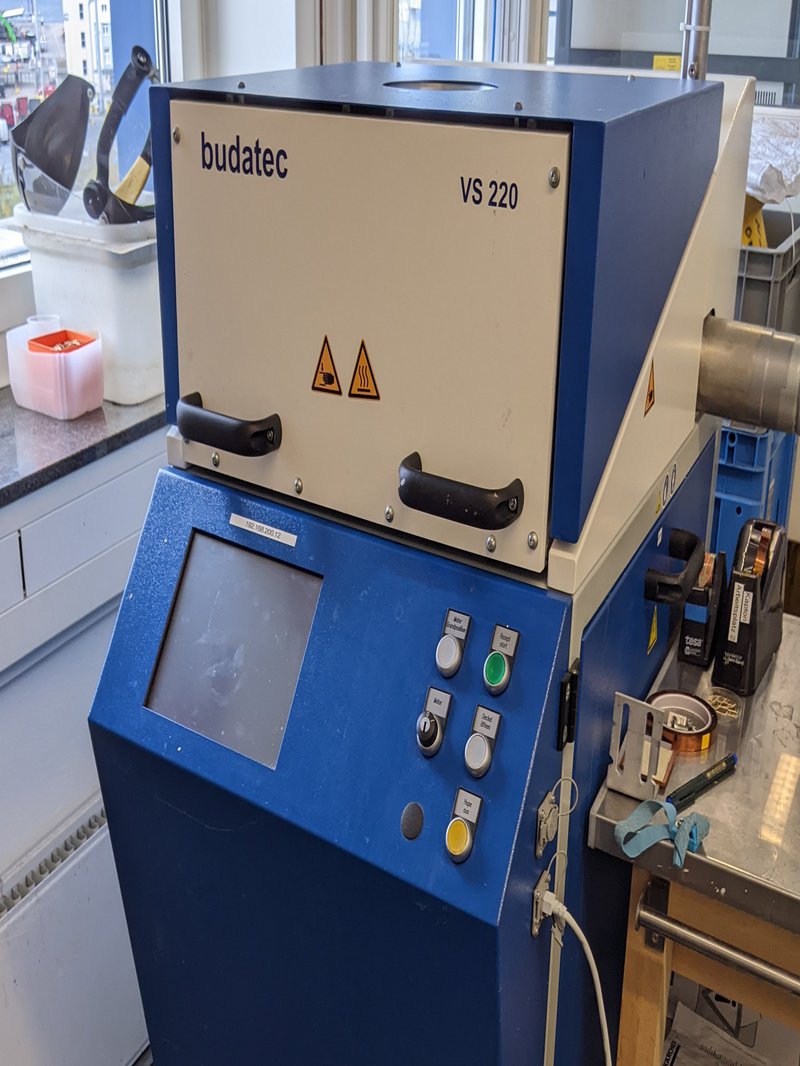
Equipment:
- Budatec SP 300
- Budatec VS 220
- 100-ton press
- Press for pressureless sintering
![[Translate to English:] Laminierpresse Collin](/fileadmin/data/iue/organisationundpersonen/mechatronik/avt/pxl_20231116_113114647.mp.jpg)
![[Translate to English:] Laminierpresse Vogt](/fileadmin/data/iue/organisationundpersonen/mechatronik/avt/pxl_20231116_113128367.jpg)
![[Translate to English:] Ofen Binder](/fileadmin/data/iue/organisationundpersonen/mechatronik/avt/pxl_20231116_113150879.jpg)
![[Translate to English:] T-Shirtpresse](/fileadmin/data/iue/organisationundpersonen/mechatronik/avt/pxl_20231116_113201579.jpg)
![[Translate to English:] Heizplatte](/fileadmin/data/iue/organisationundpersonen/mechatronik/avt/pxl_20231116_113203685.jpg)
![[Translate to English:] Vakuum](/fileadmin/data/iue/organisationundpersonen/mechatronik/avt/pxl_20231116_113217552.jpg)
![[Translate to English:] Cutter](/fileadmin/data/iue/organisationundpersonen/mechatronik/avt/pxl_20231116_113221497.jpg)
Insulating and conductive layers are bonded together to form compact, low-inductance substrates. Students learn how different materials and layer structures influence the electrical performance, thermal stability, and reliability of power modules. The focus is on both modern lamination processes and the optimization of material combinations to create efficient and durable modules.
- Electrical performance: The layers conduct electricity efficiently and reduce inductance.
- Thermal stability: Heat can be better distributed or dissipated, making modules more resilient.
- Mechanical stability: Substrates become more resistant to pressure, bending, or vibrations.
- Space savings: Multilayer laminations enable compact, lightweight modules.
- Reliability: The failure rate decreases due to clean, stable bonding of the materials.
Equipment:
- Collin laminating press, model no.: Lab Line P 300SV, compressed air 4–6 bar, water pressure 4–6 bar, max. hydraulic pressure 250 bar
- Vogt laminating press, model: LABOPRESS, water pressure 5 bar, air pressure 8 bar, max. hydraulic pressure 210 bar
- Binder laboratory oven
- T-shirt press
- Mimaki CFL-605RT flatbed cutting plotter
- Vacuum and temperature control systems
- Coating and thickness measurement devices
![[Translate to English:] Oberflächenanalyse mit dem Laser-Scanning-Mikroskop](/fileadmin/data/iue/organisationundpersonen/mechatronik/avt/_son2886.jpg)
![[Translate to English:] SAM KSI V300](/fileadmin/data/iue/organisationundpersonen/mechatronik/avt/equipment/sam.portrait.jpg)
![[Translate to English:] Keyence VR 3200](/fileadmin/data/iue/organisationundpersonen/mechatronik/avt/equipment/keyence.portrait.jpg)
![[Translate to English:] TIMA 5](/fileadmin/data/iue/organisationundpersonen/mechatronik/avt/equipment/tima.portrait.jpg)
![[Translate to English:] Keyence VHX S50](/fileadmin/data/iue/organisationundpersonen/mechatronik/avt/equipment/keyence_vhx-s50.jpg)
![[Translate to English:] Keyence VHX S750E](/fileadmin/data/iue/organisationundpersonen/mechatronik/avt/equipment/keyence_vhx-s750e.jpg)
![[Translate to English:] Keyence VKX 100](/fileadmin/data/iue/organisationundpersonen/mechatronik/avt/equipment/keyence_vkx_100.jpg)
![[Translate to English:] Thermo Fisher Scientific Phenom XL](/fileadmin/data/iue/organisationundpersonen/mechatronik/avt/equipment/phenom_xl.jpg)
![[Translate to English:] Quorum Q150R-ES-Plus](/fileadmin/data/iue/organisationundpersonen/mechatronik/avt/equipment/quorum_q150r_es_plus.jpg)
![[Translate to English:] XYZTEC Condor Sigma](/fileadmin/data/iue/organisationundpersonen/mechatronik/avt/equipment/xyztec_condor_sigma.jpg)
We systematically test power modules throughout their production chain for quality, reliability, and performance. Non-destructive methods such as ultrasonic microscopy provide insights into internal structures, while optical microscopy and material analyses examine surfaces and materials in detail. Electrical tests assess conductivity, insulation values, and dielectric strength, while thermal and mechanical tests evaluate the stress resistance of the interconnect layers and process windows.
The data obtained is directly incorporated into the optimization of design, material selection, and manufacturing processes. In this way, students learn in a practical setting how to design modern power modules that are reliable, efficient, and durable.
Optical Methods
- Digital microscopy
- Scanning electron microscopy (SEM)
- Laser scanning microscopy (LSM)
- 3D profilometer
Electrical Testing
- Determination of dielectric strength (up to 5 kV)
- Electrical testing of semiconductors (diodes, IGBTs, MOSFETs)
Thermal methods
- Thermography for hotspot analysis
- Rth measurement of substrates
- Dynamic differential scanning calorimetry (DSC)
- Thermogravimetric analysis (TGA)
- Thermal Interface Material Analyzer (ASTM D5470)
Mechanical testing
- Shear test (semiconductor and bond joints)
- Peel test / tensile test (bond joints)
- Ultrasonic microscopy (SAM)
- Mandrel bending test
Material analysis
- Energy-dispersive X-ray spectroscopy (EDX)
- Laser-Induced Plasma Spectroscopy (LIPS / LIBS)
Equipment:
- Keyence VHX-7000 with EA-300
- Keyence VHX-1000
- Keyence VR-3200
- Keyence VK-X100
- KSI V300
- Thermo Fisher Scientific Phenom XL
- Quorum Q150R ES PLUS
- Nanotest TIMA 5
- XYZTEC Condor Sigma
- GW instek GPT-12003

Bonding creates electrical connections between the chip and the substrate. This is done using fine wires or ribbons made of copper or aluminum. The bonding process is critical for current conduction and must remain stable over time—even under thermal cycling, vibration, or high currents.
Methods:
- Wedge bonder (aluminum wire): The most common method in power electronics; robust and cost-effective.
- Ball bonder (gold wire): Used primarily in microelectronics (e.g., sensors, ICs).
- Copper bonding: High conductivity, high current-carrying capacity.
- Ribbon bonding: Flat ribbons instead of round wires, reducing inductance and increasing current-carrying capacity.
Process:
- Positioning of the bonding needle.
- Ultrasonic energy, pressure, or heat create the metallurgical bond.
- Wire is tensioned, laid, and bonded at the second contact point.
Equipment:
- Orthodynde Electronics bonding machine
- Delvotec Keyboard Wirebonder
- XYZTEC bond tester
- KEYENCE digital microscopes
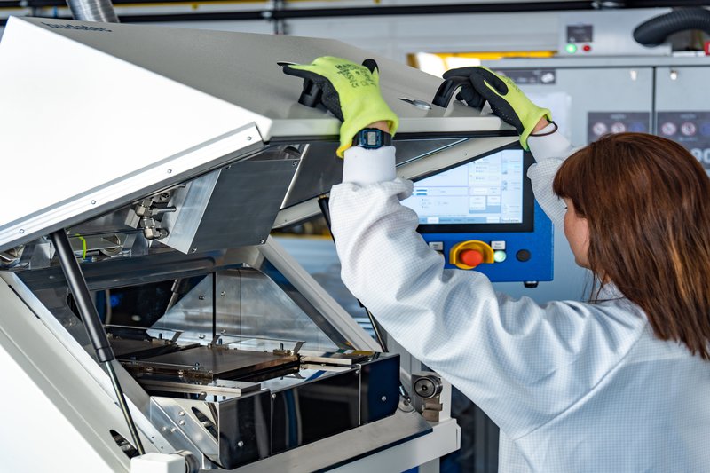
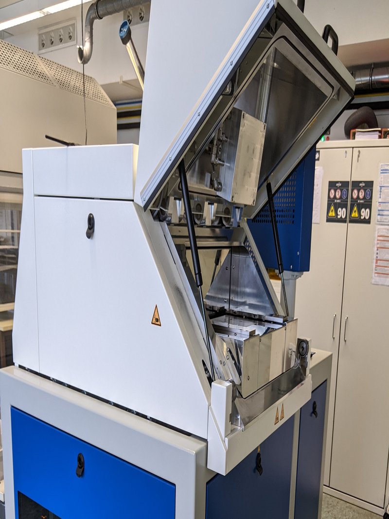
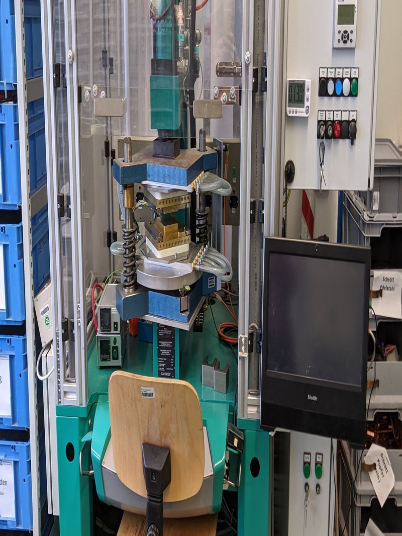
![[Translate to English:] Packaging](/fileadmin/_processed_/8/4/csm__son3075-edit_5ae574f46f.jpg)
During the packaging process, the individual components of the power module are assembled and securely embedded. Semiconductor chips, substrates, and bond connections are integrated into the housing, followed by potting or encapsulation.
The module is potted or encapsulated to protect it from moisture, dust, and mechanical stress. The choice of materials and processes directly influences service life and reliability.
This results in robust, durable modules that are protected against moisture, dust, and mechanical stress.
Equipment:
- Frame printing: Rapid prototyping
- Encapsulation
- Molding
- Potting
- Verguss
![[Translate to English:] Funktionstests](/fileadmin/_processed_/8/f/csm__son3112_fbcfe35c96.jpg)
![[Translate to English:] Schuster TLW 723](/fileadmin/_processed_/9/b/csm_schuster_ea8896af2c.jpg)
Functional tests ensure that a module actually performs as promised by the simulation. They provide hard data on electrical, thermal, and mechanical properties and are an integral part of the optimization process.
- Temperature Shock Test in Air & Fluid (TST)
- Power Cycling Test
- H3TRB
- Rth measurement of power modules / individual assemblies
- Pump-out testing of TIM material
- Deformation measurement of power modules (thermal)
Equipment:
- H3TRB test bench Schuster Elektronik HTRB 689
- Schuster Elektronik TLW 723
- Pump-out test bench
- TST test bench